| Surface Mount
PPTC - FSMD0805 Series |
|
※ RoHS Compliant / (Lead Free) Available |
| |
|
|
Application: |
All high-density boards |
| Product Features: |
Small surface mount, Solid state
Faster time to trip
than standard SMD devices
Lower resistance than standard
SMD devices |
| Operation Current: |
0.1A~1.0A |
| Maximum Voltage: |
6V~15V |
| Temperature Range: |
-40°C to 85°C |
| Agency Recognition: |
UL : E211981
TUV:
R50090556
C-UL: Pending |
|
| |
|
|
|
| |
|
Part
Number |
Hold
Current |
Trip
Current |
Rated
Voltage |
Max
Current |
Typical
Power |
Max Time
to Trip |
Resistance Tolerance |
Current |
Time |
RMIN |
R1MAX |
IH, A |
IT, A |
VMAX, Vdc |
IMAX, A |
Pd, W |
Amp |
Sec |
Ω |
Ω |
FSMD010-0805 |
0.10 |
0.30 |
15 |
100 |
0.5 |
0.50 |
1.50 |
0.700 |
6.000 |
| FSMD010-0805-R |
0.10 |
0.30 |
15 |
100 |
0.5 |
0.50 |
1.50 |
0.700 |
6.000 |
FSMD020-0805 |
0.20 |
0.50 |
9 |
100 |
0.5 |
8.00 |
0.02 |
0.400 |
3.500 |
| FSMD020-0805-R |
0.20 |
0.50 |
9 |
100 |
0.5 |
8.00 |
0.02 |
0.400 |
3.500 |
FSMD035-0805 |
0.35 |
0.75 |
6 |
100 |
0.5 |
8.00 |
0.10 |
0.250 |
1.200 |
| FSMD035-0805-R |
0.35 |
0.75 |
6 |
100 |
0.5 |
8.00 |
0.10 |
0.250 |
1.200 |
FSMD050-0805R |
0.50 |
1.00 |
6 |
100 |
0.5 |
8.00 |
0.10 |
0.150 |
0.850 |
FSMD075-0805R |
0.75 |
1.50 |
6 |
40 |
0.6 |
8.00 |
0.20 |
0.090 |
0.350 |
FSMD100-0805R |
1.00 |
1.95 |
6 |
40 |
0.6 |
8.00 |
0.30 |
0.060 |
0.210 |
|
| |
|
IH=Hold
current-maximum current at which the device will not trip at 23℃still air.
IT=Trip
current-minimum current at which the device will always trip at
23℃ still
air.
V MAX=Maximum voltage device can withstand without damage at
it rated current.(I MAX)
I MAX= Maximum fault current device can
withstand without damage at rated voltage (V MAX).
Pd=Typical
power dissipated-type amount of power dissipated by the device when
in the tripped state in 23℃ still air environment.
RMIN=Minimum device
resistance at 23℃ prior to tripping.
R1MAX=Maximum device resistance at 23℃ measured 1 hour after
tripping or reflow soldering of 260℃ for 20 seconds.
Termination pad
characteristics
Termination pad materials: Pure Tin
|
| |
|
 |
|
Part
Number |
|
A |
B |
C |
D |
E |
Min |
Max |
Min |
Max |
Min |
Max |
Min |
Max |
Min |
Max |
FSMD010-0805 |
1 |
2.00 |
2.30 |
1.20 |
1.50 |
0.55 |
1.00 |
0.20 |
0.60 |

|
|
| FSMD010-0805-R |
2 |
2.00 |
2.30 |
1.20 |
1.50 |
0.55 |
1.00 |
0.20 |
0.60 |
0.10 |
0.45 |
FSMD020-0805 |
1 |
2.00 |
2.30 |
1.20 |
1.50 |
0.55 |
1.00 |
0.20 |
0.60 |
|
|
| FSMD020-0805-R |
2 |
2.00 |
2.30 |
1.20 |
1.50 |
0.55 |
1.00 |
0.20 |
0.60 |
0.10 |
0.45 |
FSMD035-0805 |
1 |
2.00 |
2.30 |
1.20 |
1.50 |
0.45 |
0.75 |
0.20 |
0.60 |
|
|
FSMD035-0805-R |
2 |
2.00 |
2.30 |
1.20 |
1.50 |
0.45 |
0.75 |
0.20 |
0.60 |
0.10 |
0.45 |
FSMD050-0805R |
2 |
2.00 |
2.20 |
1.20 |
1.50 |
0.55 |
1.25 |
0.20 |
0.60 |
0.10 |
0.45 |
FSMD075-0805R |
2 |
2.00 |
2.20 |
1.20 |
1.50 |
0.55 |
1.25 |
0.20 |
0.60 |
0.10 |
0.45 |
FSMD100-0805R |
2 |
2.00 |
2.20 |
1.20 |
1.50 |
0.75 |
1.80 |
0.20 |
0.60 |
0.10 |
0.45 |
|
|
| |
|
 |
| |
|
|
| |
|
 |
| |
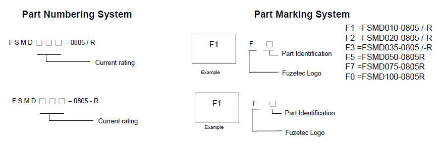
A
=FSMD010-0805/-R
B
=FSMD020-0805/-R
C
=FSMD035-0805/-R
D
=FSMD050-0805R
E
=FSMD075-0805R
F
=FSMD100-0805R
|
 |
|
| |
|

|
| |
|
 |
| |
|
| P/N |
Pcs /Bag |
Reel/Tape |
| FSMD010-0805/-R |
----- |
4K |
| FSMD020-0805/-R |
----- |
4K |
| FSMD035-0805/-R |
----- |
4K |
| FSMD050-0805R |
----- |
3K |
| FSMD075-0805R |
----- |
3K |
| FSMD100-0805R |
----- |
3K |
|
|
| |
|
| Warning: |
- Operation beyond the specified maximum ratings or
improper use may result in damage and possible electrical
arcing and/or flame.
- PPTC device are intended for occasional overcurrent
protection. Application for repeated overcurrent condition
and/or prolonged trip are not anticipated.
- Avoid contact of PPTC device with chemical solvent.
Prolonged contact will damage the device performance.
|
|
|
| |
|
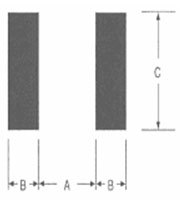
Pad
Layouts, Solder Reflow and Rework
Recommendations
The dimension in the table below
provide the recommended pad layout for each FSMD1812
device |
|
| Pad dimensions (millimeters) |
| Device |
A |
B |
C |
| Nominal |
Nominal |
Nominal |
| All 0805 Series |
1.20 |
1.00 |
1.50 |
|
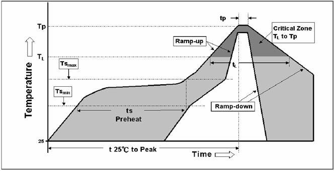
Solder
reflow
Profile Feature |
Pb-Free Assembly |
Average Ramp-Up Rate (Tsmax to
Tp) |
3 ℃/second max. |
Preheat :
Temperature Min (Tsmin)
Temperature Max (Tsmax)
|
150 ℃
200 ℃
60-180 seconds |
Time maintained above:
Temperature(TL)
|
217 ℃
60-150 seconds |
Peak/Classification Temperature(Tp)
: |
260 ℃ |
Time within 5℃ of actual Peak :
|
20-40 seconds |
Ramp-Down Rate : |
6 ℃/second max. |
Time 25 ℃ to Peak Temperature
: |
8
minutes max. |
Note 1:
All temperatures refer to of the package,
measured on the package body
surface. |
 |
Solder
reflow
※ Due to
“Lead Free” nature, Temperature and Dwelling time for the
soldering zone is higher than those for Regular. This may
cause damage to other components.
1. Recommended max past thickness > 0.25mm.
2. Devices can be cleaned using standard methods and
aqueous solvent.
3. Rework use standard industry practices.
4. Storage Environment : < 30℃ /
60%RH
Caution:
1. If reflow temperatures exceed the recommended profile,
devices may not meet the performance requirements.
2. Devices
are not designed to be wave soldered to the bottom side of the
board. |
|